Prototyping in an Hour: A Small PCB and a Quiet Shift in Embedded Work
Designing and ordering a custom PCB in under an hour — a reflection on modern KiCad workflows and how rapid prototyping has quietly changed embedded development.


With nearly two decades in electronics and embedded systems, I’ve watched PCB design change from something you planned weeks in advance to something you can do almost between meetings. This post is a short reflection on that shift centered around a small adapter board that took roughly an hour or two to design and order, start to finish.
Not because the board itself was special, but because the fact that it wasn’t special says a lot about where embedded development is today.
A Small, Annoying Problem
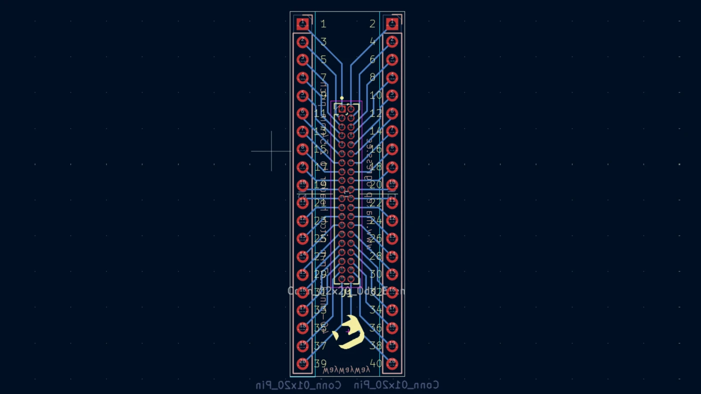
While working on an embedded display prototype project, I needed to connect a Wi‑Fi/Bluetooth module to the display board with a slightly awkward expansion header: a 40‑pin, 1.27 mm dual‑row connector. There was no off‑the‑shelf adapter that broke this out cleanly to a standard 2.54 mm pitch.

The obvious fallback would have been ribbon cable botching. It would have worked, but it would have been clumsy, fragile, and exactly the kind of workaround that tends to stick around longer than it should. For something this simple, that felt like the wrong trade‑off.
So instead of working around the problem, I designed a small board to remove it entirely.
The Board Itself
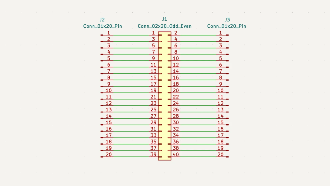
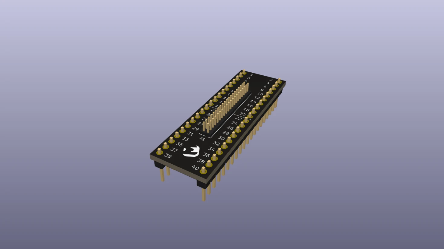
The goal was intentionally unambitious, a straight‑through adapter from a dual‑row 40‑pin, 1.27 mm header to two single‑row 20‑pin headers at 2.54 mm pitch, keeping the pin order intact on both sides. No active components, no clever routing just clean connectivity in a form factor that plays nicely with breadboards and ribbon cables.
This is the kind of board I find myself designing more and more often. Not because it’s interesting, but because it eliminates friction. And eliminating friction compounds.
Design, Without the Ceremony
I used KiCad, which has become the default tool in my workflow. The schematic was almost unimportant, one dual‑row header, two single‑row headers, wired one‑to‑one. No datasheets to cross‑check, no edge cases to reason about.
Footprint selection was equally straightforward, a 1.27 mm dual‑row pin header on one side, standard 2.54 mm headers on the other. In the PCB editor, the only real constraints were physical: spacing the 2.54 mm headers so the board would drop cleanly into a breadboard, and keeping the layout readable enough that you don’t need to think about orientation every time you plug it in.
An hour earlier, this board didn’t exist. Now it does.
From Design to Fabrication
Once the layout was done, ordering the board felt almost like buying a snack. I used PCBWay, mainly because the KiCad plugin removed nearly all friction from the handoff, upload the files, sanity‑check the preview, pick a black solder mask, and move on.
A few days later, the boards arrived alongside the rest of the development hardware, ready to be used without ceremony.

Boards like this are too small to feel like "projects", but too useful to stay buried in a local folder. The design files for this adapter live on GitHub, and I made a small batch available on Tindie for anyone who happens to run into the same header mismatch. Not because it’s a product in the traditional sense, but because sharing these small solutions reduces duplicated effort.
Wrap-Up
When designing and ordering a PCB becomes the obvious solution instead of the last resort, you start approaching embedded problems differently. You iterate faster. You accept fewer compromises. And you quietly build a library of small, purpose‑built tools that make everything else smoother.
This board isn’t special. And that’s exactly the point. ദ്ദി ˉ͈̀꒳ˉ͈́ )✧

How to Move RTT to a Custom RAM Section in Embedded Rust
Learn how to place RTT buffers and the control block into a fixed RAM section in embedded Rust. This guide covers linker script changes, custom RTT initialization, and setting up a reliable RTT print channel.
Automating OpenOCD Distribution with a Private Gitea Package Registry
Turn your OpenOCD updates from a manual chore into a one-click process. Learn how to set up a private Gitea Package Registry, upload .deb files, and install them effortlessly on any Debian-based machine. Automation made simple.

Eliminating DNS Downtime: Build a High Availability Pi-hole Cluster
Avoid DNS downtime! Learn how to set up a redundant Pi-hole system using Keepalived and VRRP. Ensure seamless failover if your primary DNS server crashes—step-by-step guide with hands-on examples.
Whether you're building something new, fixing stability issues, or automating what slows your team down — we can help.